Mendeleev to Periodic table: “Dear PT, according to you, which is the most boring element of them all?”
PT: “My Lord, Maybe copper?”
Mendeleev: “Why do you say this?”
PT: “It gets very boring for me. Unlike the other transition elements, for example iron, nickel, cobalt, which show magnetism, copper has no choice but to settle with one spin. Such monotony in spin makes it quite boring, I think.”
Mendeleev:- “Do you understand the beauty of copper? Do you know that it could change the modern electronics industry?”
PT: “No, never thought of that.”
Mendeleev: “Then listen to me carefully.
During the 1960's, Gordon Moore predicted that, in the electronics industry, the number of components that could be assembled within one integrated circuit (IC) would increase exponentially over time, and thus also the size of a fully operational IC would be reduced. Indeed, this turned out to be true in the last few decades and is expected to remain valid in the near future.
For the wiring/interconnection among the components of the ICs, a good conducting material is needed. Aluminium has been playing its role for decades. However, it is well known that copper is of better quality in terms of conductivity and resistance. If copper could replace aluminium, then it would require less space for wiring in the IC’s as well as increase its efficiency.”
PT: “Then what is the problem? I am eager to see a computer about the size of your thumb.”
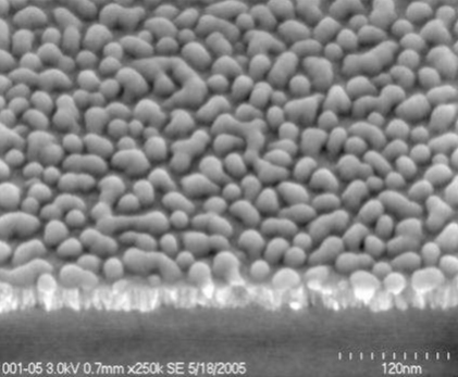
Mendeleev: “Nothing comes easy in this world. Copper follows its own chemistry regardless of whether it is located within an IC. Fellow copper atoms tend to clump together with each other and prevent the formation of a single smooth layer of copper on the surface of the semiconductor used inside the IC’s. Instead they form islands (Fig 1) consisting of few copper atoms and the height of the islands exceeds the desired thickness of an operational conducting layer. Thus, it cannot be used as a base layer for the deposition of copper. In addition, copper is poisonous to silicon as it prevents silicon from displaying its own physical and chemical properties. Moreover, there is also very poor adhesion of copper to the silicon surface.”

PT: “Is there no solution to this?”
Mendeleev :- “Scientists have tried to find a suitable glue layer like tantalum, tantalum nitride, orruthenium to which copper can bind strongly. But, so far, the surfaces have been found to be costly and not efficient enough to be used in a large scale production and are yet to be used by by a multinational semiconductor companies like Intel or IBM.”
PT: “But where do you need this copper layer?”
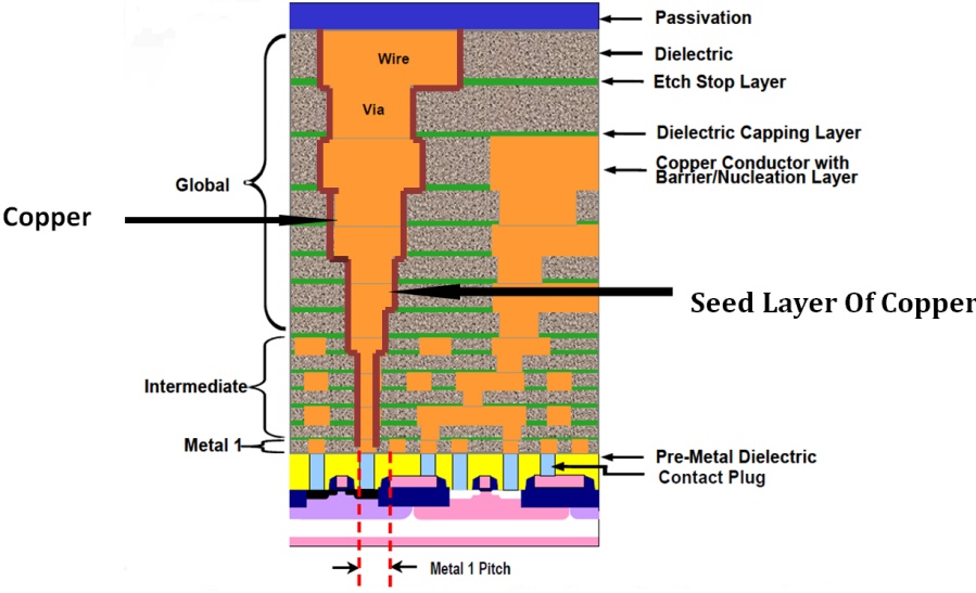
Mendeleev: “ Let me explain it to you through the schematic illustration of an interconnect as depicted in Figure 2, the whole orange portion is that of copper. It is the cross section of an interconnect. We need the copper layer over there. In order to deposit the copper very finely, we need to pass electricity. But before doing that we need a thin layer of copper which should already be present before passing the electricity to facilitate the deposition of the metal. That thin layer is known as the Seed Layer.”

PT: “How thick should the copper layer be and can it be controlled?”
Mendeleev: “The copper layer should be around 2 nm thick, or one hundredth the thickness of my hair. Such extremely thin layers can be precisely deposited for other materials by a method known as “Atomic Layer Deposition” (ALD). This method was discovered in Russia and was independently discovered again in Finland in 1970s. The ALD method works like a chemical switch, which can go on and off to build up the layers. In this way, we can get layers as thin as possible. ALD has already been extensively used in the semiconductor industry for the deposition of high-permittivity materials. There is also a big demand of this technique in many other fields.”
PT: “Can ALD be used for the deposition of copper?”
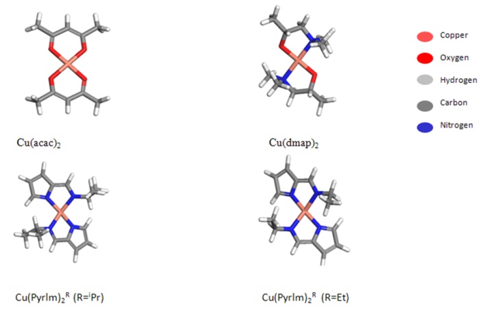
Mendeleev: “Yes, it can be, if a proper precursor molecule is found which has good attachment to the surface and also produces inactive by-products. The precursor molecule should also be cheap and usable for large scale production in the industry. If a good precursor is found which has those good qualities, it has the capability to change the face of the semiconductor world.”
PT: “Where is the solution to this problem?”
Mendeleev: “Many research groups are seeking for a way to deposit copper in thin films. One in particular is the “ALDesign” project running in Tyndall National Institute which is basically addressing this problem through computer calculations using various improved softwares. The scientists are looking at the chemical properties from the atomic level. A systematic study of the chemical properties of copper precursors and their reaction mechanism with the various reducing agents like hydrogen, alcohols, etc gives an idea of what could be a better pathway for the formation of thin films of copper to be used as a seed layer. In addition, they are also looking at some unconventional reducing agents in this field, like some organometallic reagents. We can hope that the problem will be solved soon to let the electronic industry boom.”

PT: “I have to say that copper seems to be very interesting and is not at as mundane and boring as appeared to me before.”
Mendeleev: “Tapan Gupta has written a good book stating these problems. Have a look at this book if you like. Copper Interconnect Technology (Publisher- Springer ISBN 978-1-4419-0075-3)”.
I would like to thank my supervisor Dr. Simon Elliott from Tyndall National Institute for the necessary corrections., Dr. Biswajit Santra of Fritz-Haber-Institut der MPG (Berlin) for important suggestions, Science Foundation Ireland for the funding of my PhD grant number 09.IN1.I2628, ITRS and Intel USA for the permission of the pictures.

